"Explain Like I'm 5": Printed Circuit Boards December 1, 2016 13:23
What is a printed circuit board (PCB)?
Before I answer that, let's talk about how circuits were made without PCBs. Before the advent of PCBs, people soldered components and wires right to each other, usually with the help of some sort of rigid board. For example, the technique shown below is called "turret board," where wires and parts are soldered to each other and to turrets to complete a circuit.
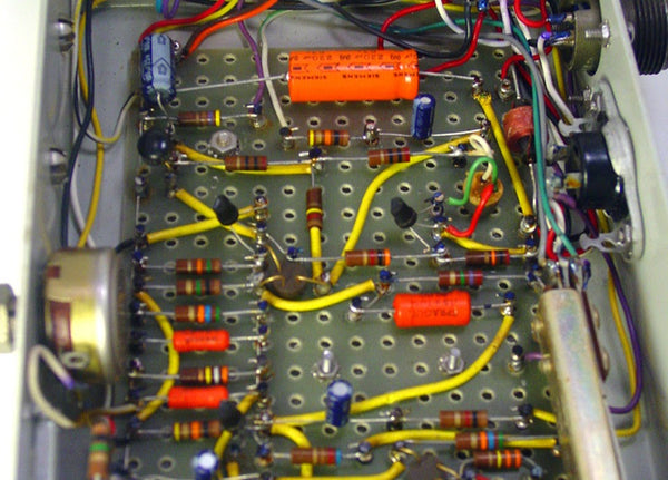
As you can see, assembling electronics used to take a lot of time, skill, and focus! Then PCBs came a long and made everything a easier by building all those wires right into the board itself.
PCBs are rigid boards with pre-wired circuitry, plus some extra perks like soldermask and silk-screening (more on those to come). So these days, instead of painstakingly cutting, bending, and soldering each connection, the assembler just has to solder each component in the right place and the PCB does the rest.
What are PCBs made of?
PCBs are made of several layers, like an onion parfait. These layers are: substrate, copper, soldermask, and silk screening. PCBs can have several of each of these layers, but most audio PCBs are "two-layer" boards (top and bottom) with this makeup:
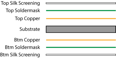
Let's take a look at a very simple PCB, our L2A Passive Re-amplifier, layer-by-layer. To keep things simple, we'll only show the top copper, soldermask, and silk-screen layers.

The core of a PCB is fiberglass. Its job is to be rigid (to hold the parts in place) and non-conductive (so electricity won't pass from one side of the PCB to the other). The holes you see in the substrate are for mounting components to the PCB.

This is where the circuit happens. The copper circles you see are called "pads"; this is where the parts get soldered to the board. The lines are called "traces"; this is what carries the electricity from one part to another. There are only a couple of traces visible here because most of them are on the bottom side of this particular PCB.

Although the pads and traces are made of the same thing, we only want to solder to the pads. So we cover the traces in a layer of polymer called "soldermask" that keeps us from getting solder on the traces.

Finally, we print some silk-screened labeling so that the humans can know where to put the parts.
Can I make my own PCBs?
Yes! Start by learning your way around an ECAD (electrical CAD) program. The most popular free programs are EAGLE, DipTrace, Upverter, and KiCad. My favorite of the bunch is Diptrace, though EAGLE is somewhat of an industry standard among DIYers. Here's what the L2A board looks like in DipTrace:

The best beginners' guide I've found to PCB layout is Dave Jone's PCB Design Tutorial (PDF).
Once you've got a layout, you can either order your PCB from a manufacturer, or etch your own at home.
OSHPark is an amazing, game-changing service that charges only $5 per square inch for three copies of your PCB. Unless you plan to make lots of PCBs at home, you won't beat that price rolling your own, and you certainly won't approach the same quality.
If you just love the idea of making your own PCBs or can't wait for OSHPark to deliver, Make Magazine has a great rundown of all the ways you can roll your own.
Any other questions about PCBs you like me to answer?
Let me know in the comments!